
The nanometer-sized graphene in the form of ribbon theoretically can control the electronic current and hold the characteristics of a semiconductor overcoming the limitation as it is normally believed that it is unable to control the current. (image: KRISS)
SEOUL, Nov. 1 (Korea Bizwire) – A joint research team of Korean and Hungarian scientists opened a new way to use graphene, often called “dream material,” as a semiconductor element by forming it nanometer-sized ribbon.
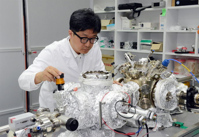
The Korea Research Institute of Standards and Science (KRISS) announced on October 30 that its Center for Nano-metrology Division led by Dr. Hwang Chan-yong and the Hungarian Center of Natural Sciences (led by Dr. Levente Tapaszto) formed a graphene nanoribbon sized from 2 to 10 nm which can control the form of edge frame freely at a room temperature. Their study results were posted on the Nature magazine, one of the most renowned science journals on the same day.
The nanometer-sized graphene in the form of ribbon theoretically can control the electronic current and hold the characteristics of a semiconductor overcoming the limitation as it is normally believed that it is unable to control the current.
The joint research team allowed the graphene nanoribbon to have the characteristics of a semiconductor by cutting the graphene into small pieces. As the nanoribbon changes its characteristics as metal or semiconductor, the precise cutting of the graphene is the key to its use as a semiconductor.
To overcome the challenges, the research team used a technology called scanning tunneling lithography (STL) and succeeded in cutting the shape of the nanoribbon edge as they wished. The technology leads the graphene’s carbon to respond to the nearby water and to form carbon dioxide by adding voltage to the graphene with a microprobe.
Besides, the research team discovered a “phase transition phenomenon” changing the graphene nanoribbon either to semiconductor or metal depending on increase or decrease in their width, which raised the possibility for its commercialization.
Dr. Hwang said, “Our research resolved the graphene’s weakness to current control and raised the possibility for graphene to be used as a semiconductor element. Also, we presented the possible usage of the graphene as a spin-off material. As our technology can produce much smaller nanoribbon than other methods, it is possible to miniaturize the semiconductor element.”
By John Choi (johnchoi@koreabizwire.com)


