
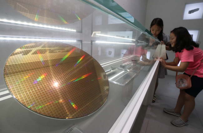
This photo taken on July 31, 2019, shows wafers displayed at an exhibition hall at Samsung Electronics Co.’s office building in Seoul. (Yonhap)
SEOUL, Nov. 18 (Korea Bizwire) — South Korea has the highest concentration of wafer capacity dedicated to advanced technology nodes, a report showed Wednesday, underscoring its leadership in the chip manufacturing sector.
The country, home to major chipmakers like Samsung Electronics Co. and SK hynix Inc., is more leading-edge focused than any other nation, with 66 percent of its wafer capacity dedicated to below 20-nanometer (nm) process geometries, according to market researcher IC Insights.
“Given Samsung and SK hynix’s emphasis on high-density DRAM, flash memory and Samsung’s applications processors, it is not a surprise that the country has the highest concentration of wafer capacity dedicated to leading-edge processes,” IC Insights said.
The market researcher added that Taiwan, home to world’s largest foundry firm TSMC, has its sub-20nm capacity standing at more than 35 percent.
A wafer is a thin slice of semiconductor substance used as a base for fabricating integrated circuits. Wafer capacity is considered a gauge for chip production by a manufacturer.
A smaller process node means finer circuitry, allowing manufacturers to make chips boasting higher speed and lower power consumption as well as producing them at lower cost per unit area.
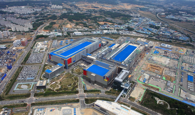
This photo provided by Samsung Electronics Co. on May 21, 2020, shows the company’s chip plant in Pyeongtaek, south of Seoul.
IC Insights said that 48 percent of all wafer capacity in 2020 is estimated to be used for devices having minimum nodes smaller than 20nm, with sub-10nm process accounting for 10 percent.
It predicted that sub-10nm process technology will continue to increase its presence down the road, with estimated shares of 22.6 percent in 2022 and 29.9 percent in 2024.
Samsung’s foundry unit can currently mass produce 5nm chips, and it plans to roll out 3nm chips in the upcoming years.
When it comes to DRAM, the company is working to produce chips with fourth-generation 10nm-class technology, also known as 1a-nm, with extreme ultraviolet (EUV) equipment.
SK hynix is currently trying to expand sales of its second-generation DRAM using 1y-nm technology, or mid-10nm class nodes. It is currently preparing to mass-produce third-generation DRAM with 1z-nm technology, or low-10nm class nodes.
The country’s No. 2 chipmaker recently said it expects to develop 1a-nm chips next year with EUV technology.
(Yonhap)


