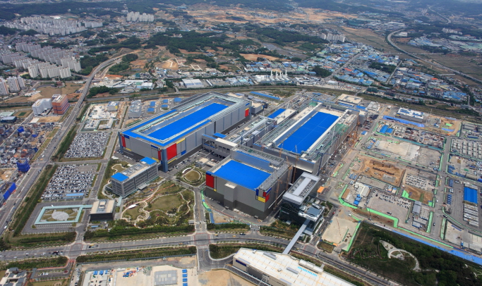
This photo provided by Samsung Electronics Co. on May 21, 2020, shows the company’s chip plant in Pyeongtaek, south of Seoul.
SEOUL, May 21 (Korea Bizwire) – Samsung Electronics Co. said Thursday it will add a foundry production line in South Korea to expand its presence in the contract chipmaking sector dominated by Taiwan Semiconductor Manufacturing Company (TSMC) Ltd. and reduce its heavy reliance on its memory chip business.
Samsung said its new foundry manufacturing line using the extreme ultraviolet (EUV) lithography technology will be established at its chip plant in Pyeongtaek, some 70 kilometers south of Seoul.
Foundry refers to the contract chip manufacturing business for fabless chipmakers that design and sell semiconductors for various types of electronics.
With the new foundry production line, Samsung will now have three foundry manufacturing facilities in South Korea. The company currently operates foundry production lines in Hwaseong and Yongin, both in Gyeonggi Province.
The world’s largest memory chip maker said it plans to start operating the new production line in the second half of 2021.
Samsung said the new EUV-equipped line in Pyeongtaek will produce chips using process nodes of 5 nanometers and below.
With the new foundry facility, Samsung will now have six foundry production lines in South Korea. The company currently operates foundry production lines in Hwaseong and Yongin, both in Gyeonggi Province.
Outside its home turf, Samsung operates a foundry production line in Austin, Texas, the United States.
“This new production facility will expand Samsung’s manufacturing capabilities for the sub-5-nanometer process and enable us to rapidly respond to the increasing demand for EUV-based solutions,” said Jung Eun-seung, president and head of the Foundry Business at Samsung Electronics.
“This will enable us to continue to break new ground while driving robust growth for Samsung’s foundry business.”
The South Korean tech titan last year unveiled a plan to become the world’s No. 1 logic chip maker by 2030 by investing 133 trillion won (US$108 billion) to bolster its competitiveness in the system LSI and foundry businesses.
According to market tracker TrendForce, Samsung took about an 18 percent share in the global foundry market in the first quarter of the year, far behind TSMC, which boasts a 54 percent share.
Samsung’s move came after TSMC said it will invest US$12 billion to build a semiconductor plant in Arizona, the United States. TSMC plans to begin operating the facility in 2024 and produce chips based on a process node of 5 nanometers.

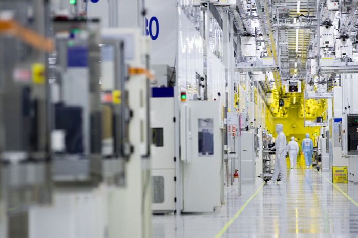
A cleanroom in a Samsung Electronics semiconductor production facility in Suwon, Gyeonggi Province. (image: Samsung Electronics)
TSMC’s decision came as the Donald Trump administration announced it will block foreign chipmakers using American equipment and software from shipping products to Chinese tech giant Huawei Technologies Co. without a license and reportedly pressured the chip company to build a plant in the United States.
There has been speculation that Samsung may expand its foundry facility in Austin, Texas, to secure its U.S. customer base following the TSMC’s move.
Samsung, however, said nothing has been confirmed about its investment plan in the U.S.
Samsung has been aggressively pushing for the adoption of EUV lithography technology for its chip manufacturing in recent years as it enables scaling down of complex patterns on wafers and allows the company to produce better quality chips for next-generation applications, such as 5G, artificial intelligence and automotive.
In 2019, Samsung became the industry’s first to begin mass-producing chips based on the 7-nanometer EUV fabrication process from its S3 line in Hwaseong.
In February, the company said its V1 line in Hwaseong, Samsung’s first chip production line dedicated to EUV lithography technology, started to produce chips using process nodes of 7 nanometers and below.
Samsung said it plans to mass-produce 5-nanometer chips in the second half of the year.
(Yonhap)


