
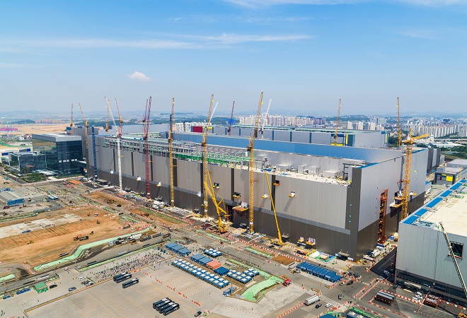
This photo provided by Samsung Electronics Co. shows the company’s P2 fab in Pyeongtaek, south of Seoul, where its NAND flash production line will be established.
SEOUL, June 1 (Korea Bizwire) — Samsung Electronics Co., the world’s largest memory chip maker, said Monday it will add a NAND flash production line in South Korea to further expand its presence in the sector.
The company said it plans to start mass-production of the new line at its second chip fab, named P2, in Pyeongtaek, some 70 kilometers south of Seoul, in the second half of 2021. It will produce Samsung’s latest V-NAND memory there.
A NAND chip is a non-volatile computer memory primarily used in memory cards and solid state drive products.
Samsung did not reveal how much money will be spent on the new line, but industry insiders estimate around 8 trillion won (US$6.5 billion).
The investment is meant to cope with rising demand for NAND flash with the emergence of artificial intelligence, Internet of Things and 5G technologies, according to Samsung.
“The new investment reaffirms our commitment to sustain undisputed leadership in memory technologies, even in uncertain times,” said Choi Cheol, an executive vice president of memory global sales and marketing at Samsung.
As the recent virus pandemic has sparked increases of non-face-to-face activities, the company expects demand for such memory to grow rapidly.
Samsung has been the global leader in the NAND flash market since 2002.
In the first quarter of this year, the company held a 33.3 percent share of the market, according to industry researcher DRAMeXchange, far above Japan’s Kioxia Corp. that took a 19 percent share.
Last July, the company mass-produced sixth-generation V-NAND memory that boasts a fast data transfer rate.
Samsung currently runs NAND flash production lines in Hwaseong and Pyeongtaek, both south of Seoul, as well as Xian, China.
The latest decision comes after Samsung decided to establish a new foundry manufacturing line using the extreme ultraviolet (EUV) lithography technology also at its P2 fab in Pyeongtaek.
Amid rising uncertainties due to the virus pandemic and renewed tensions between the United States and China, Samsung has been reinforcing its efforts to expand its chip business.
Last year, the South Korean tech titan unveiled a plan to become the world’s No. 1 logic chip maker by 2030 by investing 133 trillion won.
Samsung Electronics Vice Chairman Lee Jae-yong visited the company’s EUV-dedicated V1 line in Hwaseong in February and the Xian chip factory in China last month to inspect their business plans.
(Yonhap)
Samsung did not reveal how much money will be spent on the new line, but industry insiders estimate around 8 trillion won (US$6.5 billion).


![[FastKorea] Samsung acquires United States set-top box maker](http://koreabizwire.com/wp/wp-content/uploads/2013/07/Samsung-Smart-TV-app-370x246.jpg "[FastKorea] Samsung acquires United States set-top box maker")
