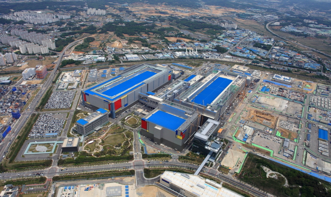
This photo provided by Samsung Electronics Co. on May 21, 2020, shows the company’s chip plant in Pyeongtaek, south of Seoul.
SEOUL, Aug. 1 (Korea Bizwire) — Samsung Electronics Co. is projected to see further growth in its foundry business in the second half of the year, analysts here said Saturday, with growing expectations for receiving orders from Intel Corp.
In its second-quarter earnings announcement, the world’s largest memory chipmaker said its foundry business achieved record quarterly and half-yearly revenues, though it did not reveal exact figures.
The South Korean tech titan added that the increase of its customers’ inventory build-ups led to robust earnings in its contract chipmaking business.
“Currently in the foundry industry, only Samsung and Taiwan Semiconductor Manufacturing Company (TSMC) can offer extreme ultraviolet (EUV) lithography technology for chipmaking,” said Lee Jae-yun, an analyst at Yuanta Securities.
“But as customers’ demand for the EUV process is soaring, it will serve as a good opportunity for Samsung’s foundry business.”
Analysts said Samsung could benefit from Intel’s plan to outsource more chip manufacturing.
Earlier this week, Intel, the world’s top semiconductor firm by sales, said it is facing delays in delivering 7-nanometer (nm) chip technology, and that it may reach out to chip foundries.
“Companies that can produce chips with 7nm technology have narrowed down to Samsung and TSMC,” said Kim Kyung-min, an analyst at Hana Financial Investment.
“Whether Intel outsources its CPU or other chipsets to any specific foundry firm, there is no winner or loser. It will bring a trickle-down effect to the foundry industry as a whole and can benefit both TSMC and Samsung.”

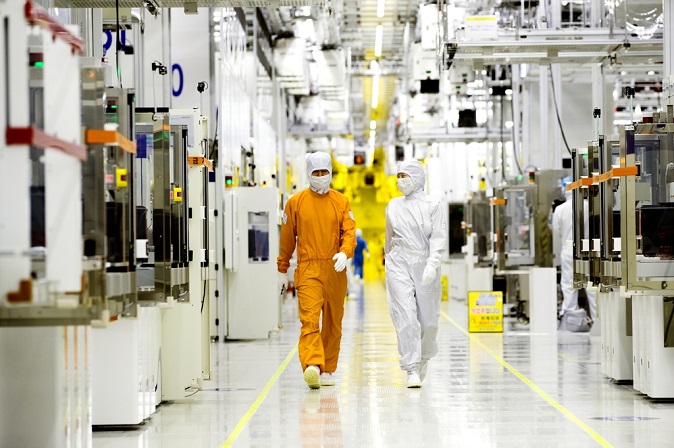
Two employees of Samsung Electronics Co. check equipment of the clean room of its semiconductor production facility in this photo provided by the company on May 15, 2019.
In the second half, Samsung said its foundry unit plans to mass-produce mobile and high-performance computing (HPC) products based on advanced process technology, while diversifying applications beyond mobile products.
Samsung has been trying to bolster its foundry capacity in recent years to catch up to the industry juggernaut TSMC.
According to market tracer TrendForce, Samsung’s share in the foundry market was estimated at 18.8 percent in the second quarter of the year, while that of TSMC was estimated at 51.5 percent.
In a conference call, Samsung confirmed it began mass production of 5nm products and is developing 4nm process technology as planned.
In May, Samsung announced it will add new foundry production line in Pyeongtaek, south of Seoul, focusing on EUV-based 5nm and below process technology. The company already has an EUV-dedicated V1 line in Hwaseong, south of Seoul.
Samsung said the adoption of EUV lithography technology is becoming important, as it enables scaling down of complex patterns on wafers and offers the best option for advanced applications such as 5G and artificial intelligence.
(Yonhap)


