(image: Teledyne e2v)
![]()
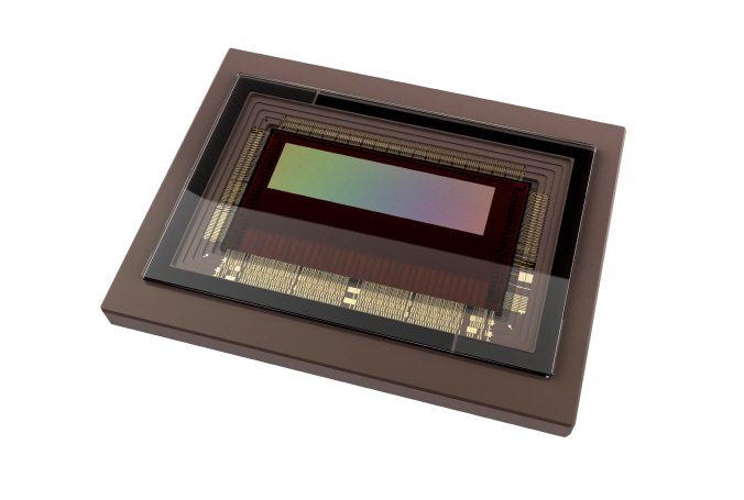
GRENOBLE, France, Sept. 3 (Korea Bizwire) – Teledyne e2v, a Teledyne Technologies [NYSE: TDY] company and global innovator of imaging solutions, announces its Flash CMOS image sensor family, specifically tailored for 3D laser profiling/displacement applications and high speed, high resolution inspection.
The new Flash sensors feature a 6μm CMOS global shutter pixel which effectively combines high resolution and fast frame rate. They are available in a 4k or 2k horizontal resolution, with respective frame rates of 1800fps and 1500fps (8 bits), and respective readout speeds of 61.4Gbps and 25.6Gbps (the best Gbps/price ratio in the market). The sensors come in a µPGA ceramic package fitting in standard optical formats, APS-like optics in the 4k and C-Mount in the 2k.
Designed to enable easy and cost-effective integration for camera makers, the new sensors include a wide range of application-based features including:
- High Dynamic Range modes with up to 100dB that enables both the measurement and inspection of highly-reflective surfaces and dark areas in the same image
- Multiple Region of Interest mode that provides the ideal tradeoff between profiling rate and range/resolution in the height measurement
- Frame to frame ‘hot’ changes mode of some parameters (exposure time, binning, ROI, flipping and conversion time) that enables flexibility and real-time adaptation to the environment conditions
- Different trigger modes that allow customers to adapt, depending on the speed of production lines
Flash image sensors are available with a wide range of derivatives at sensor level, so that customers can differentiate to meet specific applications challenges. Examples include, multiple operating modes which trade-off between frame rate, power consumption and the number of bits, increasing frame rate by utilizing horizontal binning and the capability to optimally fit the Scheimpflug angle required for your specific application.
Yoann Lochardet, Marketing Manager for 3D at Teledyne e2v said, “We are very pleased to announce the release of the new Flash family of CMOS sensors which were developed after listening closely to the requirements of leading companies in the market. These new sensors feature a unique set of characteristics targeted at 3D laser triangulation applications including; high resolution, very high frame rate, very high readout speed, HDR capability and a large set of additional features. All these capabilities allow our customers to solve the most challenging application demands in 3D laser profiling/displacement such as quality control and 3D measurement.”
Evaluation Kits and samples of Flash 2K and Flash 4K are now available. Please visit the product page or contact us for more information.
For media enquiries, please contact:
Jessica.Broom@teledyne.com | + 44 (0)1245 453607
Notes to Editors:
About Teledyne e2v
Teledyne e2v is part of the Teledyne Imaging Group. Their innovations lead developments in healthcare, life sciences, space, transportation, defence and security and industrial markets. Teledyne e2v’s unique approach involves listening to the market and application challenges of customers and partnering with them to provide innovative standard, semi-custom or fully-custom imaging solutions, bringing increased value to their systems. For more information imaging.teledyne-e2v.com
About Teledyne Imaging
Teledyne Imaging is a group of leading-edge technology companies aligned within the Teledyne brand. With unrivalled expertise across the electromagnetic spectrum and decades of experience, the group offers world-leading capabilities in sensing, signal generation and processing. The collective delivers innovative solutions to aerospace, defense, geospatial, machine and industrial vision, medical and life sciences, semiconductors and MEMs. For more information, visit teledyneimaging.com
A photo accompanying this announcement is available at https://www.globenewswire.com/NewsRoom/AttachmentNg/60d239b0-83eb-4c40-91cd-ec9be0d27603
Source: Teledyne e2v via GLOBE NEWSWIRE