
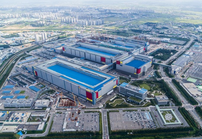
Samsung’s Pyeongtaek campus in Pyeongtaek, 70 kilometers south of Seoul, is seen in this photo provided by Samsung Electronics Co. on Sept. 7, 2022.
SEOUL, Sept. 7 (Korea Bizwire) — Samsung Electronics Co. said Wednesday it has begun operation of a new advanced, massive chip manufacturing line in South Korea.
The new production line (P3) in Pyeongtaek, the largest chip manufacturing facility ever built to date by Samsung, has started production of state-of-the art NAND flash since July.
“The Pyeongtaek campus is fast emerging as Samsung’s key manufacturing hub for cutting-edge semiconductors ranging from the world’s smallest 14-nanometer (nm) DRAM and leading-edge V-NAND to sub-5nm logic solutions,” Kyung Kye-hyun, CEO and president of Samsung’s device solutions division, said at a rare press event at the campus, some 70 kilometers south of Seoul.
The P3 line is equipped with Dutch chip equipment maker ASML’s extreme ultraviolet (EUV) lithography machines, critical to making advanced chips.
Samsung, the world’s largest memory chip maker, said it has begun foundation work for yet another manufacturing line, P4, at its Pyeongtaek’s mega 2.9 million-square-meter campus.
Home to 60,000 employees, the Pyeongtaek campus is nearly the size of the 1.45 million-square-meter Giheung campus and the 1.6 million-square-meter Hwaseong campus combined, according to Samsung.
In May, U.S. President Joe Biden toured the Pyeongtaek campus, where he emphasized the importance of semiconductors and close collaboration in the field between South Korea and the U.S.
Samsung has five semiconductor operations in South Korea — Giheung, Hwaseong, Pyeongtaek, Onyang and Cheonan — and four manufacturing sites in the United States and China — Austin, Suzhou, Tianjin and Xi’an.
It is currently building a US$17 billion plant in Austin, Texas.
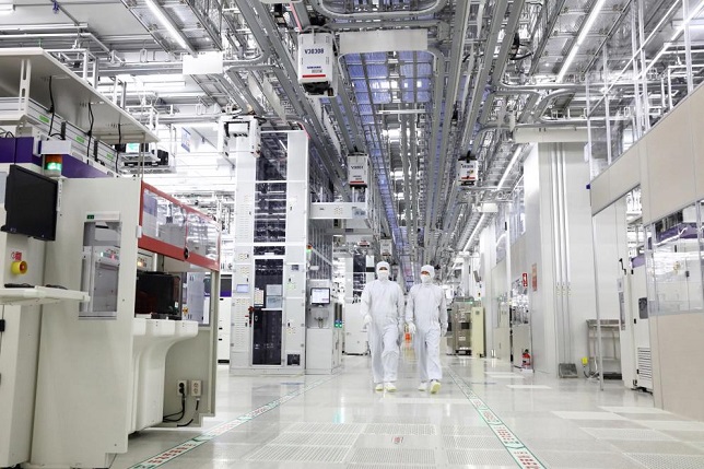
This photo, provided by Samsung Electronics Co., shows the tech giant’s new production line (P3) in Pyeongtaek, 70 kilometers south of Seoul, the largest chip manufacturing facility ever built to date by Samsung, whose production of state-of-the art NAND flash began on Sept. 7, 2022.
At the press briefing, Kyung struck a gloomy note, saying the chip industry has entered a down cycle and is facing various challenges, as the global economy has slowed and businesses tightened their spending.
“I don’t see good momentum in the second half and into the next year … but we will try to turn this crisis into a good opportunity,” he said.
In order to achieve that, investment regardless of the economic situation is crucial, he said.
“Less investment in a down cycle could lead to bad results in good times,” he said, adding “consistent investment is the right way to go.”
As a way to boost its chip competitiveness, Samsung has been carefully considering M&A options, Kyung said.
“I can’t give you details about potential targets, but we have set our priority and been reviewing our options,” he said.
(Yonhap)


