
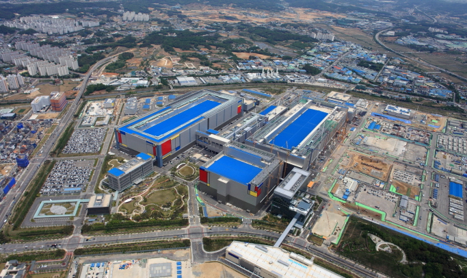
This photo provided by Samsung Electronics Co. on May 21, 2020, shows the company’s chip plant in Pyeongtaek, south of Seoul.
SEOUL, Aug. 10 (Korea Bizwire) — Samsung Electronics Co. said Thursday it will hold Memory Tech Day 2023 in October in the United States to share its newest chip technologies and products with technicians and industry officials worldwide.
The event is scheduled to take place in San Jose, California, on Oct. 20, beginning with an opening speech by Han Jin-man, president of Samsung’s U.S. semiconductor business.
The world’s largest memory chip maker uses the annual global event to unveil its latest plans for chip production and development.
During last year’s event, Samsung unveiled its fifth-generation 10nm-class (1b) DRAM, as well as eighth- and ninth-generation Vertical NAND (V-NAND), affirming what the company said was its “commitment to continue providing the most powerful combination of memory technologies over the next decade.”
At that time, it unveiled a plan to mass-produce 1b DRAM in 2023, which it claimed would “bring new capabilities to data centers, as well as the high-performance computing, mobile, gaming and automotive market segments.”
DRAM, or dynamic random-access memory, is a volatile semiconductor memory that retains data as long as power is supplied. It is commonly used in personal computers, workstations and servers.
On the NAND flash front, Samsung said it aims to mass-produce its ninth-generation V-NAND by 2024 and stack over 1,000 layers of cells by 2030.
The eighth-generation V-NAND, by far the company’s most advanced one, has 236 layers.
Adding more layers means more storage and requires more advanced technologies.
NAND flash is a type of non-volatile storage that does not require power to store data.
While the chip industry is still passing through a trough, chipmakers have been working hard to take a leading position in the field of high-performance and high-capacity semiconductors that are increasingly in higher demand in the artificial intelligence era.
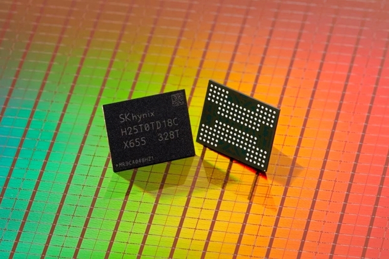
This photo, provided by SK hynix, shows a sample of the world’s first 321-layered NAND chip under development, which the South Korean chipmaker showcased at the Flash Memory Summit in Santa Clara, California, on Aug. 8, 2023.
SK hynix, the world’s second-largest memory chip maker, said Wednesday it developed what it said was the world’s first NAND flash with more than 300 layers.
At the Flash Memory Summit in Santa Clara, the world’s biggest annual conference for the NAND Flash industry, SK hynix unveiled a sample of its 321-layer 4D NAND flash.
“(The 321-layer NAND) comes with a 59 percent improvement in productivity, compared with the earlier generation of 238-layer 512Gb,” it said, “thanks to the technology development that enables the stacking of more cells and larger storage capacity on a single chip.”
(Yonhap)


