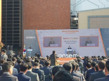
This photo provided by Samsung Electronics Co. on Oct. 7, 2021, shows an image from its foundry forum held online.
SEOUL, Oct. 7 (Korea Bizwire) — Samsung Electronics Co. on Thursday unveiled its technology road map for the foundry business as the company vowed to improve its capacity and advanced manufacturing solutions in the contract chipmaking sector.
At the Samsung Foundry Forum 2021, which was held online under the theme of “Adding one more dimension,” the South Korean chipmaker revealed its plans for future technology nodes, operations and services.
Samsung, the world’s No. 2 foundry player behind Taiwan Semiconductor Manufacturing Co. (TSMC), said it first plans to deploy gate-all-around (GAA) technology on the 3-nanometer (nm) process in the first half of 2022.
GAA refers to a modified transistor structure in which the gate wraps around all four sides of the channel for better control of current flow and further scaling. It enables significant improvement in performance with less operating power.
Samsung said it also targets to use the second-generation 3nm process in 2023 and GAA-based 2nm process in 2025 to mass-produce chips.
The company added its 3nm process node is currently on track for mass-production and it is focused on securing stable yield rates.
The tech giant said the 3nm process applied with its multi bridge channel FET (MBCFET) architecture, Samsung’s patent version of GAA technology, will be able to deliver up to a 35 percent reduction in chip area with 50 percent lower power consumption and 30 percent higher performance compared to the 5nm process with the FinFET architecture.

This photo provided by Samsung Electronics Co. on Oct. 7, 2021, shows Choi Si-young, who heads the company’s foundry business, speaking at the Samsung Foundry Forum 2021.
At the forum, Samsung also introduced the upgraded FinFET-based 17nm process with an aim to deliver more cost-efficient, applicable products.
FinFET, or fin field-effect transistor, refers to a transistor with a 3D structure. In FinFETs, three sides of the channel are surrounded by gate electrodes.
Samsung said its latest 17nm process can reduce the chip area by 43 percent, improve energy efficiency by 49 percent, and increase performance by 39 percent compared to the 28nm process.
The company said the upgraded 17nm process can also be applied to products like image sensors and mobile display integrated circuits that mainly use the 28nm process.
Samsung said it also plans to come up with various options to apply its existing 14nm node to microcontrollers.
Regarding its radio frequency technology based on the 8nm process, the company said it targets to secure the leadership in the 5G communications chip market, especially for products supporting sub-6 GHz and mmWave spectrums.
Meanwhile, Samsung, also the world’s largest memory chip supplier, said it will hold the Samsung Advanced Foundry Ecosystem (SAFE) forum in November to beef up relations with its partners and clients.
(Yonhap)


