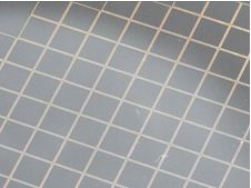
The appearance of AuRoFUSE(TM) sealing frames (200 micrometers wide) printed on an 8-inch wafer. (image: Tanaka Holdings/ACN Newswire)
Tokyo, July 29 (Korea Bizwire) — Tanaka Holdings Co., Ltd. (a company of Tanaka Precious Metals) announced today that Tanaka Kikinzoku Kogyo K.K., which operates the Tanaka Precious Metals Group’s manufacturing business, and MEMS CORE Co., Ltd. (“MEMS CORE”) have concluded a joint development agreement and committed to a technology alliance for pattern formation technology used in MEMS (microelectromechanical systems) devices using submicron-sized (one ten-thousandth of a millimeter) gold particles developed by Tanaka Kikinzoku Kogyo.
Based on this, Tanaka Kikinzoku Kogyo will transfer originally-owned submicron gold particle patterning technology and equipment to MEMS CORE, which will subsequently begin manufacturing pattern prototypes using submicron gold particles and undertaking sealing for MEMS manufacturers on November 1.
By receiving the transfer of gold particle patterning technology from Tanaka Kikinzoku Kogyo, MEMS CORE will obtain process technology forming the basis of gold particle sealing, and make its MEMS device technology and products more competitive by promoting joint development projects with Tanaka Kikinzoku Kogyo in the future. Furthermore, Tanaka Kikinzoku Kogyo aims to provide increased added value to products by choosing the provision of gold particle materials as its area of operations, and concentrating on the modification and development of materials.
The two companies’ joint development organization will enable the creation of a mounting center for fab (manufacturing facility) functions in MEMS development and the consistent provision of products from material development to device mounting for MEMS manufacturers in the future.
The creation of this business model allows customers to concentrate on the development of their own products as well as improvement of productivity. At the same time, securing outsourcing contractors for prototyping and mounting leads to the reduction of the cost of ownership of new mounting facilities related to MEMS manufacturing for MEMS manufacturers experiencing increased costs of wafer level packaging (WLP) mounting due to increased device functionality. Furthermore, the rate of technological development is expected to increase in the MEMS market, which is expected to expand further in the future.
Transfer of gold particle sealing technology and equipment
In December 2009, Tanaka Kikinzoku Kogyo announced that sealing has been made possible with the application of heat and pressure using patterns of submicron gold particles with the wire width narrowed to 10 micrometers (one millionth of a meter) in patterning using photoresist(*1), and has provided MEMS manufacturers considering gold particle sealing with product samples and material prototypes, in addition to consulting implementation of technology at no cost. As a result, the practicality of gold particle sealing has been recognized, and demand for the material provision materials has increased among MEMS manufacturers.
Meanwhile, MEMS utilizes diverse combination patterns and increasing in complexity due to the use of 3D patterns combining microscopic moving parts in addition to semiconductors such as large-scale integrated circuits (LSI) on silicon substrates. Because of this, foundries with development capabilities, equipment, and excellent processing technology unique to MEMS are required in development and the manufacturing of prototypes for supporting small lot production of a diverse range of products.
MEMS CORE, a venture company from Tohoku University (a leader in MEMS research), is a foundry which provides development support specializing in MEMS devices and other services. MEMS CORE conducts a broad range of entrusted design and development, in addition to prototyping and manufacturing through a research organization in conjunction with Tohoku University Professors Masayoshi Esashi and Shuji Tanaka. MEMS CORE has equipment for aspects spanning from the design to manufacturing of MEMS, as well as manufacturing capability supporting a variety of prototyping processes, supporting the individual development of products utilizing gold particle sealing in the future. MEMS CORE’s abundant experience in MEMS research and development is what has ultimately led to this joint development and transfer of technology and equipment.
Product overview of submicron gold particle paste
In December 2013, Tanaka Kikinzoku Kogyo began providing technology for the batch formation of complex micropatterns on substrates by employing high definition screen printing using AuRoFUSE(TM) submicron gold particle paste. Vacuum performance, or high airtightness in sealing, affects quality in the manufacturing of MEMS materials.
AuRoFUSE(TM) is a paste-type bonding material containing a mixture of gold particles within the particle diameter controlled to be submicron sized and an organic solvent. When the sealing frame is thermo-compressed (200 degrees Celsius, 100MPa), gold particle sintered compacts are strained, densified, and high-vacuum sealed(*2). Vacuum sealing using AuRoFUSE(TM) has the following characteristics.
– It is possible to form prints of micropatterns on gold (Au) film of silicon wafers and substrates for high heat-resistant and low-resistivity electrode bonding and sealing frames with excellent level difference absorption.
– The printed sealing frames can create airtight seals by densifying the structure with thermocompression bonding at 200 degrees Celsius.
– Patterns can be formed using high-definition screen printing, and processing can be reduced because there is no need to combine multiple processes such as plating, deposition and sputtering as required in the past.
– 8-inch wafer size patterns can be formed.
– AuRoFUSE(TM) enables work to be performed with minimal material loss because it can withstand repeated printing. It is believed that this will enable the effective lowering of the cost of key processes.
Furthermore, AuRoFUSE(TM) is expected to be useful in die bonding (a flip chip bonding method(*3)) for high output LEDs, laser diodes, etc. because it is possible to bond at 200 degrees Celsius with no load after chip mounting in the paste form, and because it has high heat dissipation properties after bonding.
(*1) A technique for implementing etching on printed circuit boards and processing micropatterns by using a photosensitive solvent that changes chemical resistance when irradiated with light.
(*2) Achieved a helium leakage of 1.0-13 Pa m3/s. That means the leakage was such that the pressure of 1 m3 rose by 0.0000000000001 Pascal per second.
(*3) Flip chip bonding method
A bonding method for directly mounting semiconductor chips on printed circuit boards without using wire by using protruding terminals (bumps) to bond electrodes. High luminance efficiency can be realized by mounting high-output LEDs and ultraviolet LEDs with this method.
(Source: Tanaka Holdings via ACN Newswire)


