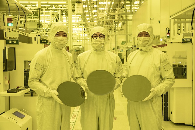
Samsung Electronics executives hold 3-nanometer semiconductor wafers in this photo provided by Samsung Electronics Co. on June 30, 2022.
SEOUL, June 30 (Korea Bizwire) — Samsung Electronics Co. said Thursday it has begun mass production of 3-nanometer semiconductors, stepping up its game in the most advanced chipmaking process node and beating its rival and foundry leader TSMC.
The next-generation 3nm chips are built on Gate-All-Around (GAA) technology, which Samsung said will eventually allow area reduction of up to 35 percent while providing 30 percent higher performance and 50 percent lower power consumption, compared with the existing FinFET process.
Samsung said its first-generation of the 3nm process node achieves a 16 percent area reduction, 23 percent higher performance and a 45 percent lower power consumption.
The advancement in the sophisticated chipmaking technology is expected to bring Samsung more customers looking for innovative and powerful semiconductors that would enable faster, more efficient technology products.
“Samsung has grown rapidly as we continue to demonstrate leadership in applying next-generation technologies to manufacturing,” Choi Si-young, president and head of Samsung’s foundry business, said.
“We will continue to develop innovative technology and work to secure a mature technology process fast,” he said.
The world’s largest memory chip maker has collaborated with its partners, including German tech firm Siemens and American silicon design company Synopsys, which are members of Samsung Advanced Foundry Ecosystem (SAFETM), since the third quarter of last year to provide its foundry customers with chip design infrastructure and other services.
The South Korean tech giant showcased its 3nm chips to U.S. President Joe Biden in May when he visited Samsung’s Pyeongtaek complex, the world’s largest semiconductor facility located some 70 kilometers south of Seoul.

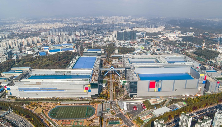
The photo provided by Samsung Electronics Co. on June 30, 2022, shows its chip campus in Hwaseong, south of Seoul.
TSMC, the world’s largest contract chip manufacturer, said it will begin mass production of 3nm chips in the second half of the year.
The two companies have been in fierce competition to outperform each other by bringing the most advanced and efficient chips to the mass market and to win customers for contract chip manufacturing.
Samsung, the world’s largest memory chip maker and second largest foundry player, has said its 2nm process node was in the early stages of development, with mass production planned for 2025.
According to industry tracker TrendForce, TSMC took up 53.5 percent of the global foundry market, followed by Samsung with 16.3 percent, in the first quarter of this year.
In 2019, Samsung unveiled a massive investment plan of 171 trillion won (US$151 billion) in the logic chip and foundry sectors by 2030, as the tech giant eyes expansion of its leadership beyond the memory business.
Last month, it unveiled additional investment plans in the chip business, vowing to cement its leading position and try to enhance its contract chip manufacturing business and create a fabless ecosystem in South Korea.
Global fabless companies, like Qualcomm, Nvidia and AMD, would want to have several stable sources to procure made-to-order chips, said Greg Roh, head of technology research at HMC Investment & Securities.
While TSMC supplies chips to Apple and AMD at the moment, Roh said it is only a matter of time before Samsung signs a deal with them to provide faster, more advanced chips than TSMC does.
“Multi-scouring is a more cost efficient and safer procurement model that reduces the risk of supply shocks,” he said.
Samsung’s foundry business is expected to grow around 40 percent this year from a year ago, compared with the estimated 25 percent growth rate of the wider industry, Roh said.
“Samsung is receiving more foundry orders than it can handle. What matters is how well and quickly the company can meet demand through long-term planning and adequate investment.”
(Yonhap)


I don’t know which is more pathetic:
Samsung’s one false start after another, which has resulted in ZERO top 20 customers, or
The stooges holding BLANK wafers (perhaps a sign of what’s to come)