
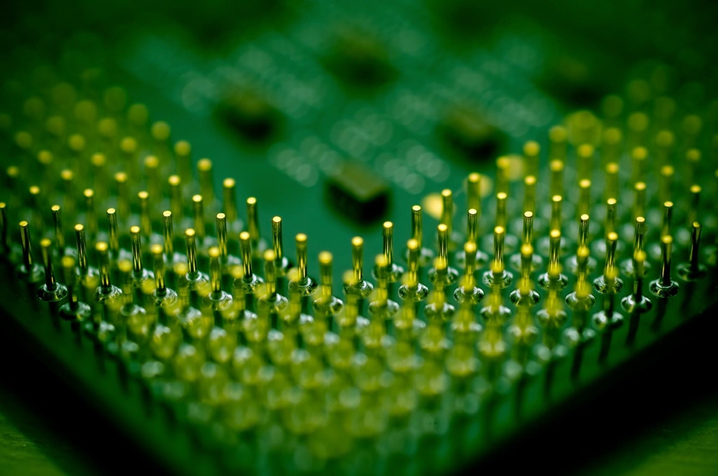
Using Lam’s advanced ALD capabilities, the latest VECTOR ALD Oxide system delivers the uniformity required for CD control of the ultra-thin films critical to SADP and SAQP schemes.(image: Lam Research)
![]()
FREMONT, CA, Jul. 13 (Korea Bizwire) – Lam Research Corp. (NASDAQ: LRCX), a major global supplier of innovative wafer fabrication equipment and services to the semiconductor industry, today announced it has released its high-productivity VECTOR® ALD Oxide system on the Extreme platform. The new product uses atomic layer deposition (ALD) to create highly conformal dielectric films with an emphasis on advanced patterning, in particular spacer-based multiple patterning. One key challenge is managing thickness variability of the self-aligned spacers that define critical dimensions (CDs). By delivering superior CD control, VECTOR ALD Oxide has been winning volume-production decisions for multi-patterning applications. Now leveraging Lam’s Extreme platform, the latest system meets productivity requirements for continued scaling, where additional steps increase process time, cost, and complexity. As a result, VECTOR ALD Oxide is gaining rapid adoption by a number of leading chipmakers for advanced multi-step patterning applications.
“Multiple patterning continues to be a key inflection for the industry, and spacer-based multi-patterning remains an enabling strategy for chipmakers for both current immersion and future EUV lithography schemes,” said Sesha Varadarajan, group vice president, Deposition Product Group. “With this in mind, we are working closely with our customers to deliver cost-effective, extendible solutions required for further scaling, such as the high-productivity atomic-scale control from our VECTOR ALD Oxide product.”
By repeating lithography/etch/deposition steps, multiple patterning techniques create smaller features and higher feature densities compared to the capability of current optical lithography using single patterning. To enable scaling for 14 nm and below, chipmakers are adopting self-aligned schemes, including self-aligned double patterning (SADP) and self-aligned quadruple patterning (SAQP), where deposition plays a critical role in forming the pattern-defining spacers. These deposition processes are challenging since they must form high-quality conformal and very uniform films. For example, a 200-300 angstrom-thick film can have only a few angstroms thickness variation across the wafer. For next-generation 10 nm processes, the manufacturing complexity will continue to increase as additional multi-patterning process steps are added, with each step contributing to overall CD variability.
Using Lam’s advanced ALD capabilities, the latest VECTOR ALD Oxide system delivers the uniformity required for CD control of the ultra-thin films critical to SADP and SAQP schemes. The quad-station modules process four wafers simultaneously and share components to improve reliability and chamber matching, contributing to industry-leading wafer-to-wafer repeatability performance. The system’s compact design delivers as much as 20% higher footprint productivity compared with other solutions. Process hardware has also been optimized to enable fast gas and RF switching, increasing throughput and reducing precursor usage for improved running costs. These innovative process module features combined with the high-productivity platform deliver the performance and cost-efficiency needed for manufacturing. Consequently, VECTOR ALD Oxide is winning development and production tool of record positions at leading manufacturers for advanced multi-patterning applications. This momentum is being successfully expanded to other applications, such as high-aspect ratio liners for through-silicon vias (TSVs) and image sensors.
About Lam Research
Lam Research Corp. (NASDAQ: LRCX) is a trusted global supplier of innovative wafer fabrication equipment and services to the semiconductor industry. Lam’s broad portfolio of market-leading deposition, etch, strip, and wafer cleaning solutions helps customers achieve success on the wafer by enabling device features that are 1,000 times smaller than a grain of sand, resulting in smaller, faster, and more power-efficient chips. Through collaboration, continuous innovation, and delivering on commitments, Lam is transforming atomic-scale engineering and enabling its customers to shape the future of technology. Based in Fremont, Calif., Lam Research is a NASDAQ-100 Index® and S&P 500® company whose common stock trades on the NASDAQ® Global Select Market™ under the symbol LRCX. For more information, please visit http://www.lamresearch.com. (LRCX-P)
Caution Regarding Forward-Looking Statements
Statements made in this press release that are not of historical fact are forward-looking statements and are subject to the safe harbor provisions of the Private Securities Litigation Reform Act of 1995. Such forward-looking statements relate to, but are not limited to, statements concerning the ability of Lam’s products to meet customer productivity requirements, the use of spacer-based multi-patterning in future EUV lithography schemes, customer requirements for future scaling, the increased complexity of next-generation 10 nm processes, and the process module features needed for manufacturing. Some important factors that may affect these forward-looking statements include the evolution of process technologies, evolving customer requirements, and novel manufacturing solutions. Such forward-looking statements are based on current beliefs and expectations and are subject to risks, uncertainties and changes in condition, significance, value and effect, including those discussed in Lam’s annual report on Form 10-K under the heading “Risk Factors” as well as in other documents filed by Lam with the Securities and Exchange Commission. Such risks, uncertainties and changes in condition, significance, value and effect could cause actual results to differ materially from those expressed herein and in ways not readily foreseeable. Readers are cautioned not to place undue reliance on these forward-looking statements, which speak only as of the dates made and of information reasonably known to Lam as of the dates the statements were made. We undertake no obligation to release the results of any revisions to these forward-looking statements which may be made to reflect events or circumstances which occur after the date hereof or to reflect the occurrence or effect of anticipated or unanticipated events.
CONTACT INFORMATION
Company Contact:
Kyra Whitten
Corporate Communications
510/572-5241
email: kyra.whitten@lamresearch.com
Source: Lam Research via Marketwired

 with 2.75M in Token Rewards")


