
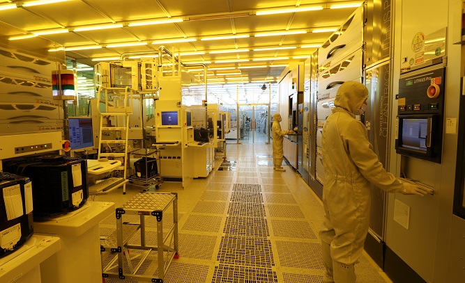
Equipment for a 12-inch semiconductor test bed is shown in this photo provided by the National Nanofab Center on March 16, 2021.
SEOUL, March 16 (Korea Bizwire) — South Korea’s ICT ministry said Tuesday a 12-inch semiconductor wafer test bed was established here in line with the country’s efforts to boost development of homegrown chip technology.
Previously, the absence of the test bed had led many local small and medium-sized chip component companies to rely on overseas testing facilities, according to the Ministry of Science and ICT.
The country’s major chipmakers, such as Samsung Electronics Co. and SK hynix Inc., require evaluations of chip components based on 12-inch wafers.
Since August 2019, the National Nanofab Center has spent 45 billion won (US$40 million) to create the test bed, made up of 10 core equipment and a clean room.
The facility will be available for use by companies, universities and research institutes starting Wednesday, according to the ministry.
The move comes as the country looks to boost its reliance on homegrown technology, following a trade dispute with Japan in 2019.
In July that year, Japan imposed tighter regulations on exports of key materials to Seoul, prompting South Korea to wean off reliance on global trade partners and boost local supply chains of technological materials.
(Yonhap)


