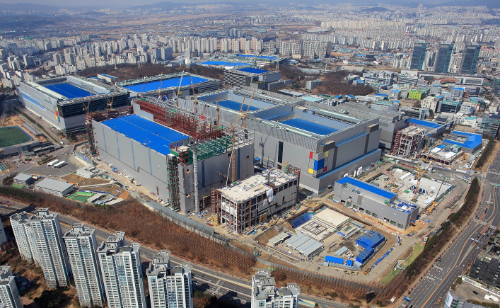
Samsung Electronics Co.’s semiconductor production line in Hwaseong, south of Seoul. (image: Samsung Electronics Co.)
SEOUL, Apr. 16 (Korea Bizwire) — Samsung Electronics Co. said Tuesday that it has completed the development of its latest fabrication process technology, bolstering its bid to expand its presence in the global foundry market.
Samsung, the world’s largest memory chip maker, said the development of its 5-nanometer (nm) FinFET process technology is complete and now is ready for customers’ samples.
The South Korean tech giant said its ultraviolet (EUV)-based process will improve performance, with an advanced cell architecture, and improve energy efficiency over its previous 7 nm, which started mass production earlier this year.
The new fabrication process technology underscores the company’s schemes for the more advanced fabrication technologies that they plan to use in various applications in the coming years.
“In successful completion of our 5nm development, we’ve proven our capabilities in EUV-based nodes,” Charlie Bae, executive vice president of foundry business at Samsung Electronics, said in a release.
“Samsung’s EUV-based advanced nodes are expected to be in high demand for new and innovative applications, such as 5G, artificial intelligence (AI), high performance computing (HPC), and automotive.”
Samsung produces its EUV chips at a production line in Hwaseong, south of Seoul, and plans to complete construction of a new line at the site in the second half. The company said it will ramp up EUV-based production from next year.
The company is accelerating its fabrication roadmap to keep up with rivals in the foundry industry, which is mostly dominated by Taiwanese manufacturers, as a way to tackle the slowing of the memory chip market, its main source of income.
According to market researcher TrendForce, Taiwan’s TSMC held 56.1 percent of the global foundry market in the first half of 2018.
Samsung, which ranked fourth with a 7.4-percent share, is actively promoting its multi-project wafer service among potential clients to explore new cooperation possibilities.
Fabless chip makers, such as U.S. tech behemoths Qualcomm and Broadcom, design and sell semiconductors for various types of electronics, but they source the work to foundries to benefit from lower capital costs.
In January, Samsung Vice Chairman Lee Jae-yong said the company aims to bolster its non-memory chip and foundry business to snatch the top spot in the sector by 2030.
(Yonhap)


