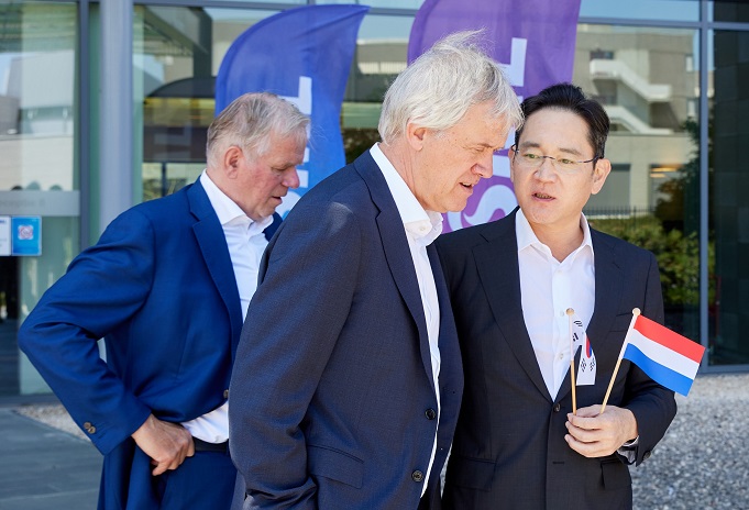
Samsung Electronics Vice Chairman Lee Jae-yong (R) talks with ASML CEO Peter Wennink at the Dutch chip equipment maker’s headquarters in Veldhoven, the Netherlands, on June 14, 2022, in this photo provided by the company.
SEOUL, June 15 (Korea Bizwire) – Samsung’s de facto leader Lee Jae-yong discussed ways to boost cooperation in the semiconductor business with ASML CEO Peter Wennink, the company said Wednesday.
Samsung Electronics Vice Chairman Lee, who is currently on a business trip in Europe, met with Wennink and CTO Martin van den Brink at the chipmaker’s office in Veldhoven, the Netherlands, on Tuesday (local time) to talk about ways to expand chip cooperation and the procurement of ASML’s extreme ultraviolet (EUV) lithography systems, which are essential to the production of advanced chips, according to Samsung.
Lee was accompanied by Samsung Electronics Co-CEO Kyung Kye-hyun, who is in charge of the company’s chip business.
Top executives of the two chip companies exchanged opinions on the future trend of chip technology, the industry’s outlook and cooperation in advanced semiconductor manufacturing technology, Samsung said.
Lee visited ASML in October 2020 to discuss supply plans of EUV equipment essential for producing chips with the 7-nanometer process or below.
The two tech firms, among the world’s most important players in the chip industry, have been working closely for many years. But they are now seen stepping up their partnership amid the global chip shortage and a growing chip demand.
In April, Wennink visited South Korea for a chip cluster project and meetings with local employees as the company is expanding its Korean operations.
The last time Wennink visited the country in November, he met with Samsung and SK hynix executives to discuss chip development and supply issues.
On the same day, Lee also met Dutch Prime Minister Mark Rutte to talk about ways to expand chip cooperation and solve global supply chain problems.
The Netherlands is an important market and home to many advanced semiconductor companies, such as ASML and NXP.
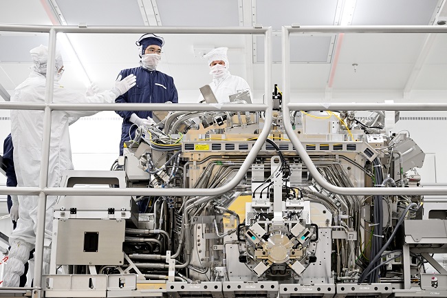
Samsung Electronics Vice Chairman Lee Jae-yong inspects a chipmaking machine at the Dutch chip equipment maker ASML’s factory in Veldhoven, the Netherlands, on June 14, 2022, in this photo provided by the company.
On Wednesday, Lee met with Luc Van den hove, CEO of imec in Belgium, a semiconductor and nanotechnology research center and a leading developer of advanced chip technology.
Imec, in particular, works with ASML on advanced lithography.
Lee toured the company and was briefed on the center’s nanotechnology, artificial intelligence and biotechnology, Samsung said.
Lee left for the Netherlands, Germany and France on June 7, his second overseas business trip in six months. In December, he visited the United Arab Emirates and Saudi Arabia to expand global networks and seek new business opportunities.
Lee’s trip came two weeks after the South Korean tech giant announced a massive investment plan for the next five years to sharpen its competitiveness in the chip industry.
Samsung said it will invest 450 trillion won (US$355 billion) in semiconductors and biopharmaceuticals in the span of five years, 80 percent of which will be used for research and development and nurturing talent in South Korea, especially in advanced chipmaking.
In particular, the company said it will import the EUV machines at an early date, which it said “will give Samsung an advantage in making the most advanced microchips.”
He is set to return home Saturday.
(Yonhap)


