
- Korean engineers have developed a 10-nanometer ultra-fine printing technology for the first time in the world that can print high-performance smart sensors on a mass-production basis(Image: KAIST)
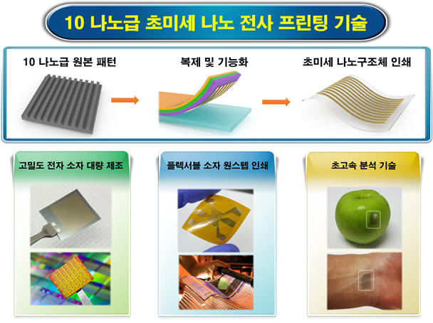
SEOUL, Nov. 13 (Korea Bizwire) — Korean engineers have developed a 10-nanometer ultra-fine printing technology for the first time in the world that can print high-performance smart sensors on a mass-production basis. Theoretically, the Tripitaka Koreana, a 13th-century collection of the Buddhist scriptures carved onto more than 80,000 wooden blocks, can be condensed onto an A4-sized paper with the 10-nm ultra-fine printing technology.
This newly invented technology was developed by a research team consisting of Dr. Park Jae-hong from the National Nanofab Center, Dr. Lee Seung-yong from KAIST, and Prof. Jung Yeon-sik from KAIST. The joint study was conducted under the leadership of Prof. Jung, and the team developed the technology that 10-nm nano-structure can be copied into any type of material to print out.
If this newly invented technology is in practical use, cutting-edge goods can be produced on a mass-production basis without complicated process. Before this technology is developed, only several hundred nano meter printing was available due to adhesive problem between materials.
It was commonly held that a 10-nm nanometer ultra-fine printing technology was theoretically impossible. However, the joint engineering team used a high-density molecule mold that made ultra-fine printing possible instead of the usual ordinary elastic mold.
With this found, the team was able to print out under 10-nm ultra-fine nano-structure, and the team devised a specific technique to selectively weaken the adhesion of surface of the elastic mold so that the nano-structure can be copied onto the surface of almost every material.
Moreover, the team successfully stamped the 10-nm nano-structure not only to a silicon wafer board but also to human skin. The 10-nm technology made possible a high-performance gas sensor to detect explosive gas immediately. Also the team invented a sensor that detects an infinitesimally small amount of agricultural pesticide found in produce.
The team’s next goal is to reduce the detection time to a few seconds and bring out to the market in the future. Prof. Jung said that this will be the core technology for the next 10 years and the global market will expand to $100 billion as various cutting-edge appliances can be developed using this technology.
By Caroline Seo (caroline@koreabizwire.com)


