
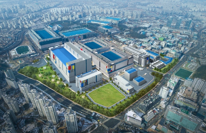
A computer-generated image of Samsung Electronics Co.’s fabrication line in Hwaseong, south of Seoul. (image: Samsung Electronics Co.)
SEOUL, Apr. 22 (Korea Bizwire) — South Korea’s major chipmakers are stepping up efforts to expand their presence in the foundry and non-memory businesses to diversify portfolios that heavily rely on memory chips in search of new growth engines, industry officials said Monday.
Samsung Electronics Co. and SK hynix Inc. hold over 60 percent of the world’s memory market with their competitive edge in DRAM and NAND chips, but they have been grappling with slowing global demand after a two-year super cycle.
The sluggish performance by the world’s top two memory makers is not only bad news for the companies but also poses a challenge for Asia’s fourth-largest economy, which relies heavily on exports.
Semiconductor exports accounted for about 20 percent of the nation’s total exports in 2018, prompting the government to expand support for the key export industry.
Last month, President Moon Jae-in urged the government and the industry to come up with measures to develop the foundry and non-memory sector to ease the nation’s dependence on the memory chip business.
The latest move also comes as China is bolstering its bid to develop its own semiconductor industry and cut its heavy dependence on foreign imports.
As the government is preparing comprehensive measures to develop the semiconductor ecosystem with increased support for the foundry and non-memory segment, Samsung is expected to announce its investment plan for the promising sector when senior policymakers visit its Hwaseong plant, south of Seoul, later this week, according to company officials.
In January, Samsung Vice Chairman Lee Jae-yong said the company aims to bolster its non-memory chip and foundry business to snatch the top spot in the sector by 2030.
According to global research firm Gartner, the value of the non-memory chip market was estimated at $346.6 billion last year — 65 percent of the total — more than twice that of the memory chip sector.
Non-memory chips comprise a broad range of semiconductor products, including processors, chipsets and image sensors.
Foundry refers to the contract chip manufacturing business for fabless chip makers, such as U.S. tech behemoths Qualcomm and Broadcom, which design and sell semiconductors for various types of electronics.
According to market research firm TrendForce, Taiwan’s TSMC held 56.1 percent of the global foundry market in the first half of 2018. Samsung, which ranked fourth with a 7.4 percent share, is actively promoting its multi-project wafer service among potential clients to explore new cooperation possibilities.
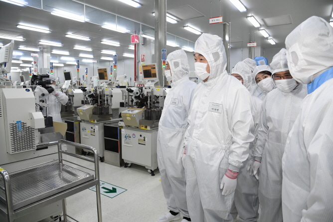
Lee Nak-yon (2nd from L), South Korea’s prime minister, visits SK hynix Inc.’s Chongching factory in southwestern China on March 29, 2019. (Yonhap)
Samsung has been actively promoting its latest nanometer fab technology based on extreme ultraviolet lithography (EUV).
The nanometer measurement, which is a key metric in the semiconductor fabrication business, is an indicator of the space between transistors on a chip. The smaller the size, the more challenging and expensive the chips generally are to develop and deploy, leaving only a few companies available for clinching deals for advanced chips.
Last week, the company said the development of its 5-nanometer (nm) FinFET process technology is complete and now ready for customer samples. It said the EUV-based process will improve performance and energy efficiency over its previous 7-nm technique, which started mass production earlier this year.
Both Samsung and TSMC have been working on a 7-nm process node meant to serve as a foundation for the next generation of processors.
“Samsung’s EUV-based advanced nodes are expected to be in high demand for new and innovative applications such as 5G, artificial intelligence, high performance computing and automotive,” Charlie Bae, executive vice president of foundry business at Samsung Electronics, said in a release.
Its smaller rival, SK hynix, which mostly earns revenue from DRAM and NAND flash, is also jacking up investment in non-memory technologies, including image sensors.
Last week, SK hynix said it has completed the expansion of its fabrication line in China’s Wuxi to step up its DRAM production.
The project worth 950 billion won (US$833 million) began in 2017 to expand the Wuxi factory’s production capacity to meet growing demand for DRAM, which is used in servers and computers.
The Wuxi fab has been in operation since 2006 and currently accounts for about 50 percent of SK Hynix’s DRAM production.
The company has been also focusing on developing CMOS image sensors designed for the automotive market to provide higher speed and superior image quality for vehicles.
In February, the chipmaker announced a plan to spend 120 trillion won to build a semiconductor cluster in Yongin, south of Seoul, to maintain its competitive edge in the global market.
Four semiconductor fabrication plants will be built at a site in Yongin, starting in 2022, which would make it the world’s largest semiconductor cluster.
(Yonhap)


