
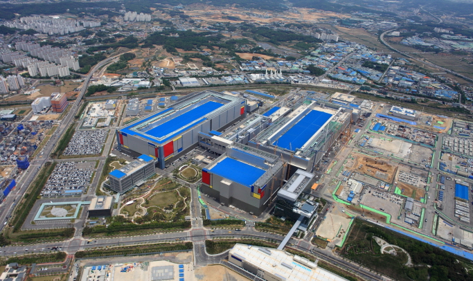
This photo provided by Samsung Electronics Co. on May 21, 2020, shows the company’s chip plant in Pyeongtaek, south of Seoul.
SEOUL, Aug. 10 (Korea Bizwire) — Samsung Electronics Co. will start the construction of its third chip fabrication facility in South Korea next month at the earliest, industry insiders said Monday, as the company tries to ramp up its production capacity to cope with rising demand for semiconductors.
Land preparation work for the facility in Pyeongtaek, south of Seoul, has been taking place since June, but the construction of a building is expected to commence in September, according to the city government and Samsung.
Samsung apparently wanted to build Pyeongtaek Line 3, better known as “P3,” earlier than scheduled, according to the city officials, as the company asked authorities to grant a construction permit quickly.
P3 is reportedly going to be Samsung’s biggest chip fabrication facility in Pyeongtaek. The world’s largest memory chipmaker plans to build a total of six chip fabrication facilities at the Pyeongtaek complex.
More than 30 trillion won (US$25.2 billion) is expected to be spent for building P3.
The company is currently running P1 and is preparing to fully operate P2 next year. Considering manufacturing equipment settings and testing period, industry insiders speculate that mass production at P3 could begin in the second half of 2023.
Samsung has not confirmed the production schedule and what kind of chips P3 will produce.
“It is difficult to specify when the facility will bring chip manufacturing equipment and start production,” a Samsung official said. “The schedule could be adjusted depending on the situation of the semiconductor market.”
Samsung’s aggressive push for the chip business comes after it unveiled a vision to become the world’s No. 1 logic chipmaker by 2030 by investing 133 trillion won and bolstering its competitiveness in the system LSI and foundry businesses.
Samsung Electronics Vice Chairman Lee Jae-yong, the de facto leader of Samsung Group, also has been emphasizing the importance of technological prowess in the chip industry while visiting the company’s semiconductor facilities in South Korea and China.
According to Pyeongtaek officials, Samsung is pushing to build another three chip fabrication facilities quickly as the company recently requested that the city secure more industrial water for construction.
“It takes some time to secure industrial water, so Samsung moved in advance to cope with its construction plan,” an official from the Pyeongtaek municipal government said.
“As far as I know, the construction of P4, P5, P6 facilities will proceed step by step under the plan.”
(Yonhap)


