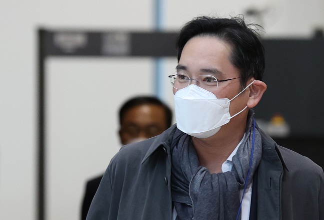
Samsung Electronics Vice Chairman Lee Jae-yong arrives at Gimpo International Airport in Seoul following his business trip to Europe on Oct. 14, 2020. (Yonhap)
SEOUL, Oct. 14 (Korea Bizwire) — Samsung Electronics Vice Chairman Lee Jae-yong, the de facto leader of South Korea’s top conglomerate, returned home Wednesday after meeting with top executives from ASML Holding N.V., the world’s leading photolithography equipment maker, in the Netherlands.
Lee met with ASML CEO Peter Wennink and ASML Chief Technology Officer Martin van den Brink at ASML headquarters in Eindhoven, the Netherlands, on Tuesday before returning to South Korea, Samsung said.
Lee departed for Europe last Thursday, making his overseas business trip for the first time in five months. He was accompanied by Kim Ki-nam, who heads Samsung’s chip business.
Samsung, the world’s largest memory chip producer, said Lee discussed with ASML executives on supply plans of extreme ultraviolet (EUV) equipment essential for producing chips with the 7-nanometer process or below, cooperation in advanced semiconductor manufacturing technology and the industry outlook amid the COVID-19 pandemic.
He also visited ASML’s plant to inspect its EUV equipment production.
Lee previously met Wennink and other ASLM officials in South Korea in November 2016 to discuss chip manufacturing solutions. They also had a meeting in Paris in February 2019.
Samsung has been cooperating with ASML since 2000 to boost its competitiveness in semiconductor manufacturing. In 2012, the South Korean tech giant even made a strategic investment in ASML.
Samsung is trying to beef up its chip fabricating capability with EUV technology.
The advanced lithography solution enables the drawing of finer circuitry, meaning more data can be stored within the same surface area and more logical gates are able to fit inside a single chip, thus providing better performance and energy efficiency.
“EUV lithography is an essential technology to make advanced chips used for artificial intelligence, 5G and autonomous driving applications,” the company said. “Samsung and ASML have been working together to solve technical issues related with EUV technology.”
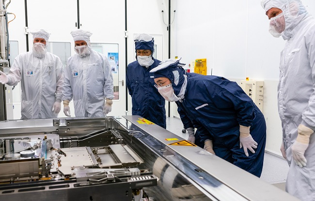
This photo provided by Samsung Electronics Co. on Oct. 14, 2020, shows Samsung Electronics Vice Chairman Lee Jae-yong (2nd from R) inspecting ASML’s EUV equipment for semiconductor manufacturing at ASML’s plant in Eindhoven, the Netherlands, on Oct. 13, 2020.
Lee’s visit comes at a time that Samsung is seeking to boost its presence in the non-memory sector.
Samsung last year unveiled a plan to become the world’s No. 1 logic chip maker by 2030 by investing 133 trillion won (US$115 billion) to bolster its competitiveness in the system LSI and foundry businesses.
According to market researcher TrendForce, Samsung had a 17.4 percent share in the global foundry market in the third quarter, far behind industry leader Taiwan Semiconductor Manufacturing Co. (TSMC), which posted a dominant 53.9 percent market share.
Samsung recently bagged foundry deals from Nvidia and Qualcomm, allowing it to catch up to TSMC. The company also commenced the construction of a new foundry line in Pyeongtaek, South Korea, that is focused on EUV-based 5-nanometer and below process technology.
Meanwhile, Lee also visited the International Olympic Committee in Lausanne, Switzerland, during his trip to Europe.
Samsung did not reveal why Lee visited the IOC, but industry officials speculated that it could be related with the company’s sponsorship of the Olympic Games.
Samsung Electronics is the sole South Korean company to have The Olympic Partner (TOP) status, the highest grade in the Olympics sponsorship program.
It has been a sponsor of the Olympics since 1988, and it recently extended the partnership deal with the IOC until 2028.
(Yonhap)


