
Choi Si-young, head of the foundry business at Samsung Electronics Co., delivers a keynote address during the Samsung Foundry Forum in San Jose, California, on June 12, 2024, in this photo provided by the company. (Image courtesy of Yonhap)
SEOUL, Jun. 13 (Korea Bizwire) — Samsung Electronics Co. said Thursday it will provide comprehensive “one-stop” artificial intelligence solutions for its foundry customers, with a focus on up-to-date technologies for high-performance, low-power AI chips.
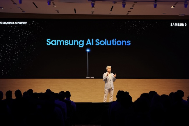
“At a time when numerous technologies are evolving around AI, the key to its implementation lies in high-performance, low-power semiconductors,” Choi Si-young, head of foundry business at Samsung Electronics, said during the annual Samsung Foundry Forum (SFF) in San Jose, California.
“Alongside our proven gate-all-around (GAA) process optimized for AI chips, we plan to introduce integrated, co-packaged optics (CPO) technology for high-speed, low-power data processing, providing our customers with the one-stop AI solutions they need to thrive in this transformative era.”
At this year’s SFF, the South Korean tech firm unveiled its foundry business road map, highlighting its technological innovations and visions for the AI era.
Samsung AI Solutions is a turnkey AI platform resulting from collaborative efforts across the company’s foundry, memory and advanced package (AVP) businesses.
Samsung Electronics is uniquely positioned as the only company with all three semiconductor businesses, allowing it to offer customer-tailored solutions in a single deal.
The company said it plans to introduce an all-in-one, CPO-integrated AI solution in 2027, aiming to provide customers with one-stop AI solutions.
Additionally, Samsung Electronics announced new foundry process nodes, SF2Z and SF4U, for its latest 2 nanometer and 4nm processes to meet the booming demand for AI chips and compete with Taiwan Semiconductor Manufacturing Co. (TSMC), the world’s leading foundry.
SF2Z, the company’s latest 2nm process, incorporates optimized backside power delivery network (BSPDN) technology to enhance power, performance and area for better high-performance computing designs. The mass production of SF2Z chips is scheduled to begin in 2027.
TSMC had earlier announced plans to apply BSPDN technology to its 1.5nm process by 2026.
Furthermore, Samsung Electronics said its SF4U technology for optical shrink will be applied to its 4nm process, with mass production planned for 2025.
Samsung Electronics said its preparations for the cutting-edge 1.4nm process are progressing “smoothly,” with performance and yield targets on track for mass production in 2027.
(Yonhap)


