
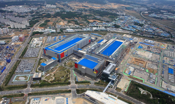
This photo provided by Samsung Electronics Co. on May 21, 2020, shows the company’s chip plant in Pyeongtaek, south of Seoul.
SEOUL, May 13 (Korea Bizwire) — Samsung Electronics Co. announced Thursday that it will invest a total of 171 trillion won (US$151 billion) in the logic chip and foundry sectors by 2030 as the tech giant eyes to expand its leadership beyond the memory business.
The latest investment plan expands its semiconductor vision announced in 2019, when it pledged to invest 133 trillion won. Samsung, the world’s largest memory chip producer, decided to spend an additional 38 trillion won to achieve its goal of becoming the world’s No. 1 logic chip maker by 2030.
Its expanded investment came as the country aims to establish a supply chain amid global semiconductor shortage woes.
The government plans to offer tax incentives and state subsidies for semiconductor companies to spend a combined 510 trillion won by 2030.
Samsung’s plan also follows its rivals’ move to increase production capacity to meet soaring demand for semiconductors.
Taiwan Semiconductor Manufacturing Co. (TSMC) recently announced that it will invest $100 billion over the next three years for capacity expansion.
The world’s top contract chip maker already unveiled last year it would set up a $12 billion plant in Arizona, the United States, but speculation has been growing that the company may build five additional fabs.
Intel Corp., the world’s leading semiconductor seller, also announced that it will invest $20 billion to expand its chipmaking capacity and teased its re-entry to the foundry business.
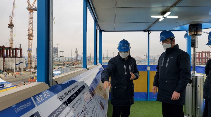
This file photo provided by Samsung Electronics Co. on Jan. 4, 2021, shows Samsung Electronics Vice Chairman Lee Jae-yong (R) checking the construction of the company’s third chip manufacturing factory in Pyeongtaek, south of Seoul.
Samsung is currently planning to build a new chip facility in the United States believed to be focused on foundry. The company already runs a foundry fab in Austin, Texas, but it is looking to build another to catch up with the industry leader TSMC.
TSMC led the foundry sector with a dominant 56 percent market share, while Samsung trailed behind with an 18 percent share in the first quarter, according to market researcher TrendForce.
With its upgraded investment plan, Samsung said its new chip fabrication plant in Pyeongtaek, south of Seoul, will be completed in the second half of 2022.
Pyeongtaek Line 3, better known as P3, will produce seventh generation 14-nanometer DRAM chips and 5-nanometer logic semiconductors using extreme ultraviolet (EUV) lithography technology, according to the company.
Land preparation work for P3 already started in September. Samsung said its Pyeongtaek Campus will be the world’s leading semiconductor cluster and will serve as a supply base for advanced chip products.
Samsung, meanwhile, also vowed to expand its support to local partners and parts suppliers to build a healthy ecosystem for the logic chip and foundry sectors, saying its upcoming investments will also lead the growth of domestic fabless companies.
(Yonhap)


